


.jpg "banner4")
.JPG "banner3")


Sophisticated Analytical Instruments Facility
| Name of the equipment/facility: Fluorescence Spectrophotometer | 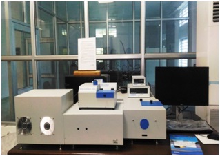 |
| Make: Horiba | |
| Model: Fluorlolog-3 | |
| Specification: | |
Excitation Source : 450W ozone free steady state and UV Xenon arc lamp and pulsed XE Lamp for phosphorimetry placed in the same housing and required power supplies. An additional port for laser excitation of sample to be provided in the sample chamber. Excitation Monochromator : Automated double monochromator, 300 nm blazed, continuously adjustable slits. Excitation Range : 200-950 nm; band pass 0-15 nm Emission Monochromator (L-Channel) : Automated double monochromator, blazed at 500 nm, continuously adjustable slits Emission Range : 200-950 nm; band pass 0-30 nm Wavelength accuracy : +/- 0.5 nm Integration time : 1 ms – 100 s or better Detector for L- Channel : Red sensitive PMT, 250-850 nm, capable of measuring steady state fluorescence, steady state and time resolved phosphorescence Reference Detector : Photodiode Reference Sensitivity : Signal to Noise ratio: 6000:1 (in L-channel) Sample Holder : Normal 1 cm cell holder and Quartz NMR tube holder for phosphorescence measurements, Solid sample holder : Designed for viewing front face flurescence of thin films, powders, pellets, fibers or microscopic slides, variable alignment angle. Multiwell-Plate Reader Module : 96 Well and 364 wells microplates. Sample Chamber :Versatile sample chamber with facilityfor liquid nitrogen cooling and gas purging facility for phosphorescence measurement Front face excitation :Front face excitation (22.5 0C) facility for solid samples for detection in L-channel TCPSC upgrade : NanoLED lifetime upgrade (NanoLED mount for sample chamber, DeltaHYB timing electronics, NanoLED Controller, software amplifier/discriminator, 30ps lifetime with TBX/PPD detectors, 200 ps lifetime with R928 detector (NanoLED dependent), NanoLED sample compartment with NanoLED. TCSPC Sources : Pulsed LED with peak WL 280nm +/- 10nm : Pulsed LED with peak WL 330nm +/- 10nm : Pulsed LED with peak WL 370nm +/- 10nm : Pulsed LED with peak WL 455nm +/- 10nm : Pulsed LED with peak WL 570nm +/- 10nm : Pulsed LED with peak WL 605nm +/- 10nm |
|
| Working Principle: | |
| Applications: | |
| Molecules have various states referred to as energy levels. Fluorescence spectroscopy is primarily concerned with electronic and vibrational states. Generally, the species being examined has a ground electronic state (a low energy state) of interest, and an excited electronic state of higher energy. Within each of these electronic states there are various vibrational states. In fluorescence, the species is first excited, by absorbing a photon, from its ground electronic state to one of the various vibrational states in the excited electronic state. Collisions with other molecules cause the excited molecule to lose vibrational energy until it reaches the lowest vibrational state of the excited electronic state. This process is often visualized with a Jablonski diagram. The molecule then drops down to one of the various vibrational levels of the ground electronic state again, emitting a photon in the process. As molecules may drop down into any of several vibrational levels in the ground state, the emitted photons will have different energies, and thus frequencies. Therefore, by analysing the different frequencies of light emitted in fluorescent spectroscopy, along with their relative intensities, the structure of the different vibrational levels can be determined. For atomic species, the process is similar; however, since atomic species do not have vibrational energy levels, the emitted photons are often at the same wavelength as the incident radiation. This process of re-emitting the absorbed photon is "resonance fluorescence" and while it is characteristic of atomic fluorescence, is seen in molecular fluorescence as well. In a typical fluorescence (emission) measurement, the excitation wavelength is fixed and the detection wavelength varies, while in a fluorescence excitation measurement the detection wavelength is fixed and the excitation wavelength is varied across a region of interest. An emission map is measured by recording the emission spectra resulting from a range of excitation wavelengths and combining them all together. This is a three dimensional surface data set: emission intensity as a function of excitation and emission wavelengths, and is typically depicted as a contour map. |
|
| User Instructions: | |
| (A).Make sure that ROOM TEMPERATURE is 17-18 ºC. (B).Switch on the “FAN” first and allow to run for 5 min. (C.)Then switch on the LAMP and allow to run for 7-10 min. (D).Next switch on the SPECTRA CQ assembly and allow to run for 10-15 min. Strictly follow the above order and maintain proper time gap between each step. (E).Next start the computer and start the software i.e. FluorEssence and then initialize the hardware components by clicking initializing bouton. Be patient during the operation and do not perform other operations. (F) Placed the sample in sample compartment and proceed according to your experimental parameters. (G) While recording Excitation-emission spectrum be sure that lower limit of emission wavelength is greater than excitation wavelength by 20 nm; while upper limit is less than double of the excitation wavelength by 20 nm. e.g. if excitation wavelength is 350 nm, then emission should be recorded in between 370-680 nm. (I) After completion of measurements, immediately close the SOFTWARE first, then SPECTRA CQ and then the LAMP. Allow to run the FAN for 10-15 min after switching off the LAMP. (J)Do not keep the LAMP on unnecessarily for a long time as it reduces the LAMP life time. (K) Switch off the all the connections from power source after completion of the measurement. (L) Do not put any liquid, solvent, sample inside the sample compartment. (M) Do not try to alter the alignment of the instrument. (N) If face any problem, do not try to resolve yourselves, instead inform the competent authority at the earliest. |
|
| Contact | |
| Division: Analytical Chemistry Group, CSTD 1. Mr Hemanta Shankar Dutta,Scientist, hsdutta@neist.res.in, 7597585991 2. Dr Anil Singh, Scientist, anil@neist.res.in, 8876954752 |
|
| Charges (Excluding Taxes) | |
| (a) For National Labs( R&D) : 1000/-sample (b) University/Educational Institutes : 1000/- sample (c) Industry : 1200/- sample |
|